DNA Origami Places Quantum Emitters on Chips with 90% Accuracy: How It Works
Scientists have used DNA origami to place quantum light emitters on chips with 90% accuracy and a mean positioning precision of 13 nanometers. The research, published in the journal Light: Science and Applications on March 20, 2026, was carried out by an international team from Nanjing University, Skolkovo Institute of Science and Technology, and LMU Munich. It addresses one of the most persistent practical problems in building quantum computing and communication hardware: getting individual light-emitting components to sit exactly where they need to be on a chip, reliably and at scale.
This article explains what DNA origami is, what single-photon emitters do, why precise placement on a chip is difficult, and what the research team actually achieved.
What Is DNA Origami?
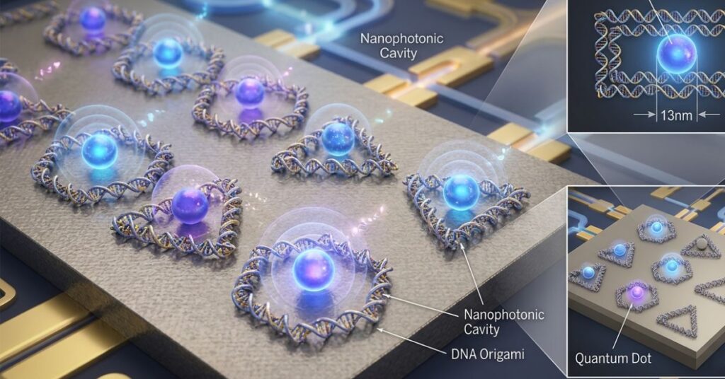
DNA origami is a technique that uses the natural pairing properties of DNA to fold long strands of genetic material into precise two-dimensional or three-dimensional shapes at the nanoscale. The name comes from the Japanese art of paper folding: just as a sheet of paper can be folded into a recognizable shape, a long DNA strand can be guided into a specific geometric structure by short complementary strands called staples.
The resulting structures are extremely small. A typical DNA origami shape measures between 50 and 100 nanometers across. For reference, a human hair is approximately 80,000 nanometers wide. At that scale, DNA origami structures are useful as molecular scaffolds, meaning they can hold other molecules or materials in precise positions.
In this research, the team used DNA origami triangles embedded with thiol molecules. Thiol is a chemical group that bonds strongly to sulfur, which is a component of the semiconductor material used in the study. By placing thiol molecules at specific points on the DNA triangles, the researchers created a programmable template that could attract and anchor quantum emitters at defined locations.
What Is a Single-Photon Emitter?
A single-photon emitter is a light source that releases exactly one photon at a time when triggered. This is different from a conventional light source such as an LED or laser, which releases large numbers of photons simultaneously.
Single photons are central to quantum communication and quantum computing because they can carry quantum information. In quantum communication, individual photons can be used to transmit encryption keys in a way that is fundamentally secure: any interception of the photon disturbs its quantum state and becomes detectable. In quantum computing, photons can serve as carriers of quantum bits, or qubits.
The challenge is that building reliable, controllable single-photon emitters that can be integrated into a chip at scale has been technically difficult. Most fabrication methods produce emitters whose positions cannot be precisely controlled, which makes it hard to build consistent, repeatable quantum devices.

What Is MoS2 and Why Was It Used?
MoS2 stands for molybdenum disulfide. It is a two-dimensional semiconductor material, meaning it can be grown or deposited as a layer that is just one or a few atoms thick. Materials at this thickness behave differently from their bulk equivalents and can display quantum optical properties that thicker versions do not.
When a single-atom-thick layer of MoS2 is placed on a surface that has been prepared with thiol molecules, the thiol groups bond to sulfur vacancies in the MoS2 lattice. A sulfur vacancy is a point where an atom is missing from the regular crystal structure. When a thiol binds to that vacancy, it creates a localized defect site that can trap excitons.
An exciton is a bound pair consisting of an electron and the positively charged hole it leaves behind when excited by energy. When an exciton recombines at a defect site, it releases a single photon. This is the mechanism by which MoS2 on a thiol-patterned surface produces single-photon emission.
What the Research Team Did: Step by Step
- Step 1: The team synthesized DNA origami triangles and embedded thiol molecules at specific, programmed positions within the triangle structure.
- Step 2: These DNA origami triangles were deposited onto a chip surface in an ordered array. The geometry of the triangles determined where the thiol groups would end up on the surface.
- Step 3: A monolayer of MoS2 was transferred onto the patterned surface. The thiol groups in the DNA templates bonded with sulfur vacancies in the MoS2 layer, creating localized defect sites at the positions defined by the DNA origami.
- Step 4: These defect sites acted as single-photon emitter locations. By adjusting the spacing of the DNA patterns, the team could control both the number of emitters formed and their positions on the chip.
- Step 5: The team measured the optical performance of the resulting emitters and confirmed single-photon emission through a metric called the second-order photon correlation function, or g(2)(0). Values below 0.5 confirm a single-photon source. The team reports values well below this threshold.
Key Results from the Study
| Metric | Result |
| Emitter placement yield | Approximately 90 percent |
| Mean positioning accuracy | Approximately 13 nanometers |
| Photon emission lifetime | Nanosecond scale (stable) |
| Single-photon confirmation | g(2)(0) values well below 0.5 threshold |
| Signal stability | Minimal blinking and photobleaching observed |
| Materials used | MoS2 monolayer, DNA origami triangles, thiol molecules |
| Institutions involved | Nanjing University, Skoltech, LMU Munich |
| Published in | Light: Science and Applications (March 20, 2026) |
Why 90% Yield Matters
In semiconductor and quantum device fabrication, yield refers to the percentage of sites where a component forms correctly out of all attempted sites. Conventional methods for creating single-photon emitters in 2D materials typically rely on random defect formation, which offers limited control over where emitters appear. This means that on a given chip, some areas will have emitters and many others will not, and there is no reliable way to predict placement.
A 90% yield using the DNA origami method means that 9 out of 10 targeted sites on the chip produced a functioning single-photon emitter. Combined with a mean positioning accuracy of 13 nanometers, this represents a level of deterministic control that conventional fabrication approaches have not achieved for this material system.
For quantum devices to move from laboratory demonstrations to manufacturable products, this kind of repeatable, high-yield placement is a necessary step. A chip where emitters appear randomly cannot be scaled reliably. A chip where emitters appear at 90% of intended positions, within 13 nanometers of their target coordinates, can form the basis for a consistent manufacturing process.
Spectral Stability: Why Blinking and Photobleaching Are Problems
Two optical behaviours have historically limited the practical use of quantum emitters in 2D materials: blinking and photobleaching.
Blinking refers to intermittent switching between bright and dark emission states. An emitter that blinks on and off unpredictably cannot be used as a reliable light source in a quantum circuit. Photobleaching refers to permanent loss of emission caused by photochemical degradation, where prolonged exposure to light damages the emitter and reduces or eliminates its output.
The emitters produced in this study showed stable optical performance with minimal blinking and photobleaching. This indicates that the thiol-bond stabilization mechanism at the MoS2 defect sites produces emitters that are physically and chemically more stable than those created by random defect methods.
Compatibility with Larger-Scale Manufacturing
The fabrication approach used in this study is compatible with wafer-scale production. A wafer is the large disc of semiconductor material on which many chips are fabricated simultaneously in industrial processes. Methods that work only at small laboratory scales cannot directly translate to commercial manufacturing.
Because DNA origami templating is a solution-based process, it can in principle be applied across a large surface area in a single deposition step. The researchers state that their method could be extended to wafer-scale integrated quantum photonic circuits, though this remains a goal for future work rather than a demonstrated result in the current study.
The platform also supports further tuning. Changing the number, type, or arrangement of molecules in the DNA templates can modify the optical properties of the emitters, including photon purity and the ability to produce chiral quantum light, which refers to light whose polarization rotates in a specific direction.
Frequently Asked Questions
What is DNA origami used for in this research?
In this study, DNA origami was used as a nanoscale template to position thiol molecules at specific coordinates on a chip surface. These thiol groups then bonded with a monolayer of MoS2, creating single-photon emitter sites at the locations defined by the DNA structure. The DNA origami acts as a programmable placement guide rather than as a functional part of the final device.
What is a single-photon emitter used for in quantum computing?
Single-photon emitters are used in quantum computing and quantum communication as sources of individual photons that can carry quantum information. In photonic quantum computing, photons serve as qubits. In quantum key distribution, single photons are used to transmit encryption keys in a way where any eavesdropping is physically detectable. Reliable, chip-integrated single-photon emitters are a building block for both applications.
What does 13 nanometers of positioning accuracy mean in practice?
13 nanometers is approximately 130 times smaller than the wavelength of visible light. It represents the average distance between where a quantum emitter was intended to be placed and where it actually formed. For comparison, the transistors in a modern smartphone chip are currently around 3 to 5 nanometers in size. A 13-nanometer positioning accuracy is precise enough for integration with nanophotonic waveguides and other chip-scale optical structures used in quantum devices.
Is this technology ready for commercial quantum chips?
The current study is a proof-of-concept demonstration. The researchers have shown that the approach works at laboratory scale and that the fabrication method is in principle compatible with larger-scale manufacturing. Commercial quantum chip integration would require further development, including demonstration at wafer scale, integration with existing chip fabrication processes, and long-term stability testing under operating conditions.
Which institutions conducted this research?
The research was conducted by an international team from Nanjing University in China, the Skolkovo Institute of Science and Technology in Russia, and Ludwig Maximilian University of Munich (LMU Munich) in Germany. The study was published in the journal Light: Science and Applications on March 20, 2026.